How to Handle Warped PCBs During Assembly
Warped PCBs During Assembly
When a PCB gets warped it becomes difficult to handle and it can cause many issues during assembly. These issues can include incorrect placement of components, missing components, solder bridges, and more. The problem can happen to your PCB during the fab and assembly processes or your components could be warped in their packaging.
The most common cause of warping is due to uneven thermal expansion between different layers of the pcb printed circuit board assembly laminate and copper. This is exacerbated when the different layers have unequal thicknesses. The most important factor in preventing thermal expansion mismatch is to distribute the copper areas evenly across the surface of the board.
PCBs are fabricated from multiple materials such as resin, glass cloth, and copper foil. Each of these materials have different properties and will respond to temperature changes differently. During fabrication, the boards are pressed together under high pressure. This pressure creates thermal stress between the layers and the material binders. Unless the material properties are exactly matched, this stress can result in warping during the reflow process.
How to Handle Warped PCBs During Assembly
To avoid warping, it is important to have a uniform stackup that does not exceed the maximum reflow temperature. The layer thicknesses should also be as close as possible to each other. In addition, the flexure of the copper layer should be minimized. This can be achieved by using thicker layer substrates and by minimizing the copper area on the edges of the PCB.
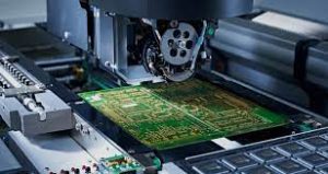
A reflow oven heats the board to extremely high temperatures which can affect its material properties and change its shape. If the PCB is not flat, it may be difficult to place SMT parts on the bare board. They may not land on the intended pads and may fall off or short to other conductive areas of the board. A warped PCB will be even more problematic when it is passed through a pick and place machine or a wave solder machine. These machines are designed for flat boards and will not be able to operate properly on one that is warped.
Fabricators often use panelization to improve assembly efficiency by combining multiple printed circuit boards into a single unit. These panels are typically held in a fixture that has rails and outriggers to facilitate handling throughout the assembly process. However, if the outriggers are not properly designed and installed, they can interfere with the alignment of the PCBs. This can lead to warping because of the difference in the copper density between the outrigger and the PCB surface area.
As a result of warping, the height of the through-hole holes will be uneven. This can affect the solder paste printing, especially for close-pitch ICs. It can also affect reflow soldering and stress the component. This can ultimately lead to fatigue failure of the component and/or solder joints or the PCB laminate itself.